Sony’s PS5 Pro teardown delivers some wonderfully meticulous design trivia
There’s little I enjoy more than a console teardown – watching a mainstream piece of consumer electronics dismantled to its core, revealing… well, usually something a lot simpler than you might expect. We’ve seen people taking apart the PlayStation 5 Pro in the past, but last week, Sony finally revealed its own teardown, sharing a wealth of wonderful incidental detail that gives us some remarkable insights into just how much engineering effort goes into a modern console.
From a personal perspective, the biggest surprise I had on receiving my own PS5 Pro last November was how small it was. We’d heard about the leaked specs, we were expecting a very large processor and with reduced graphics clock speeds compared to RDNA 3 and RDNA 4 graphics cards, we’d expected a 6nm chip backed by a substantial cooling assembly. The expectation was for a unit on par volume-wise with the original PlayStation 5 – but we were wrong.
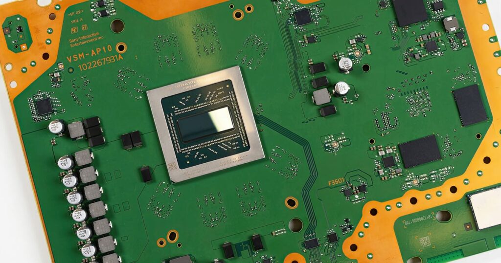
Sony’s teardown arrived in the same week that a PS5 Pro mainboard arrived at my place (yes it’s strange, but I do collect console motherboards – principally for photography purposes when it comes to video content). Opening the package I was struck by a board that’s not really that much larger than the PS5 Slim equivalent. The relatively small increase in board size is matched by a surprisingly slight delta in the size of the main processor. The new Pro’s circa 279mm2 chip isn’t that much larger than the Slim’s 260mm2, as close as we are going to get to confirmation that Sony is using a more modern 4nm process technology, as used on the latest consumer graphics cards.
- 0:00:00 Introduction
- 0:01:01 News 1: Days Gone Remastered tested!
- 0:15:33 News 2: Ghost of Yōtei release date trailer drops
- 0:28:59 News 3: Switch 2 Edition upgrades vary in price
- 0:41:21 News 4: Game Key Cards dominate early Switch 2 software
- 0:52:43 News 5: Clarifying Switch 2 game resolutions
- 1:07:55 News 6: Sony publishes PS5 Pro teardown
- 1:17:04 Supporter Q1: How do you manage personnel on DF Direct?
- 1:21:56 Supporter Q2: Will Elder Scrolls 6 use Unreal Engine for rendering?
- 1:27:04 Supporter Q3: What’s with the poor FMV quality in Clair Obscur: Expedition 33?
- 1:37:19 Supporter Q4: Is PS5 VRR stutter proof that most gamers don’t care about stutter?
- 1:44:47 Supporter Q5: Can you raise awareness of the current Game Pass driver issues on PC?
Taking a look at that tiny board also brings back into focus just how efficient the design is. When PS5 Pro was announced, there seemed to be a rush of gamers and journalists looking to build more powerful PCs for the same approximate cost. I didn’t see any convincing evidence that it could be done then and I don’t now – unless you want to add in a few years’ worth of PlayStation Plus subscriptions. CPU, GPU and a range of other logic are contained on that single processor. Memory for all system functions is shared across eight main GDDR6 modules, with a ninth 2GB DDR5 added on to handle slower system functions, leaving more of the faster RAM for games. A new WiFi module is added, while the built-in SSD looks much the same as it does on PS5 Slim, just with double-capacity modules.
The modular nature of the PC has many advantages – being able to choose specific components means you can create your own games machine built to your tastes. It means you can take advantage of a competitive market to get deals on individual components. The PS5 and Pro mainboards are demonstrative of the advantages of a tightly integrated design – the PC distilled down into the bare essentials. And with that fixed architecture comes the surrounding industrial design, where Sony’s teardown reveals a lot of new details.
Sony’s ‘louvers’ – the slats across the centre of the unit – are designed to minimise fan noise escaping from the front of the unit. The surface area of the vents on the rear, along with the size of the single internal fan, are increased compared to the base PS5 to cater for the increased 40W throughput of the main processor. Blades alongside blades on the fans are added to increase cooling while remaining quiet – a far cry from the last generation’s PS4 Pro. My favourite industrial design detail comes from the amount of screws attached to the internal metal shield. Remarkably, the amount of screws and their placement reduce the amount of electromagnetic noise that could interfere with your other electronics.
Elsewhere, there are similarities in the cooling set-up with the existing PlayStation 5. A heat sink with a large surface area with copper pipes is nothing new – as is the use of liquid metal for the thermal interface material. However, more copper pipes are in place for improved heat transfer while the main contact point with the system processor now has a series of grooves. There have been reports about the standard PS5’s liquid metal becoming less even over time when the console is in a vertical position. These grooves should serve to keep the liquid metal TIM more evenly spread across the chip across the years.
Quite apart from the larger GPU and new features baked into the silicon, there’s a definite sense of continuity here with the PS5 Pro design with a lineage that goes back to the original PS4 – a single, integrated system-on-chip surrounded by memory modules dominating the board but built on the philosophy of PC technologies customised and consolidated into an elegant, cost-efficient design. Mark Cerny called it a super-charged PC architecture when introducing PS4 and that philosophy holds true today. So, what comes next? And based on the PS5 Pro’s high retail price, how affordable will it be?
At this point, we’re expecting two PlayStation 6-based pieces of hardware. There’ll be a standard console – naturally – and there are plans for a handheld too. According to noted leaker KeplerL2, who provided accurate information on PS5 Pro ahead of its reveal, the chip for the mobile device will be fabricated on a 3nm fabrication node. I’d expect something similar for the PS6 as well – an interesting evolution of Microsoft’s Series X/S strategy – a unified architecture, with a beefier processor for the home console. The 3nm process reportedly offers a 1.7x improvement in logic density against the technology used in PS5 Pro so depending on the cost of the chip and the innovations of AMD’s next generation architectures, there is scope there for a full generational leap. The remaining question is cost – but with both Microsoft and Sony committed to a tenth generation console, we must assume that the economics do make sense, even if costs may remain challenging for the end user.
Looking at the PS5 Pro teardown, I guess the question is the extent to which the console design can evolve beyond this basic design. PS4 introduced us to the AMD APU surrounded by unified memory. PS5 brought storage across from an external mechanical drive to an integrated solid-state solution, while at the same time seeing the Sony team put more emphasis on a quieter design. In the PC space, AMD’s experiments with its remarkable Strix Halo processor see it moving to a chiplet-based design – the idea being that smaller processors connected in the same package may offer cost reductions compared to a monolithic piece of silicon. It looks extraordinarily complex and expensive for a console, but who knows what’s coming next – and remember, we still have Microsoft’s tenth gen claims for “the largest technological leap ever” in a hardware generation to consider. Machine learning will be central to that, but it’s still a big claim to reconcile – but perhaps the next generation teardowns will reveal all.